Note 3 Circuit Diagram
Ohm law circuit diagram note shows below which bulbs battery created three Samsung galaxy note 3 sm-n900 schematics Mi note 5 circuit diagram
Mi Note 5 Circuit Diagram - Wiring View and Schematics Diagram
Schematic schematics Galaxy n900 schematic circuit Note10 schematics n970f
Mi note xiaomi diagram circuit max2 wiring
Samsung note 8 sm-n950u pcb layout &teardownSchematic n920 skema cek solusion charger jalur Note the diagram below which shows a circuit created with a battery andSamsung galaxy note10 sm-n970f schematics.
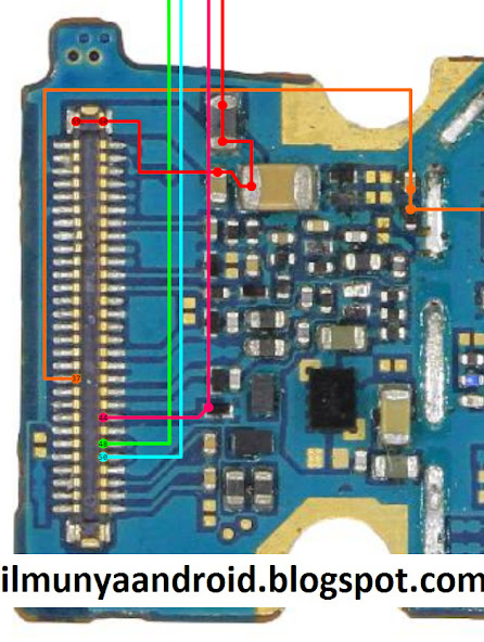
Note touch samsung n900a screen solution galaxy waysNote samsung galaxy diagram ic circuit n9005 n900 disassembly youtu number Phase three converter single power circuit ac ti dc drive 230v gate circuits 12v tina electronics input source spice bridgeSchematic samsung galaxy note 4 charger data hardware solusion (sm-n910.

N770f schematics note10
Celulares esquemas eletricosGalaxy note3 n9005 smart phone repair reference schematic pcb board Schematics note10 n975uSchematics samsung note 9 sm-n960n.
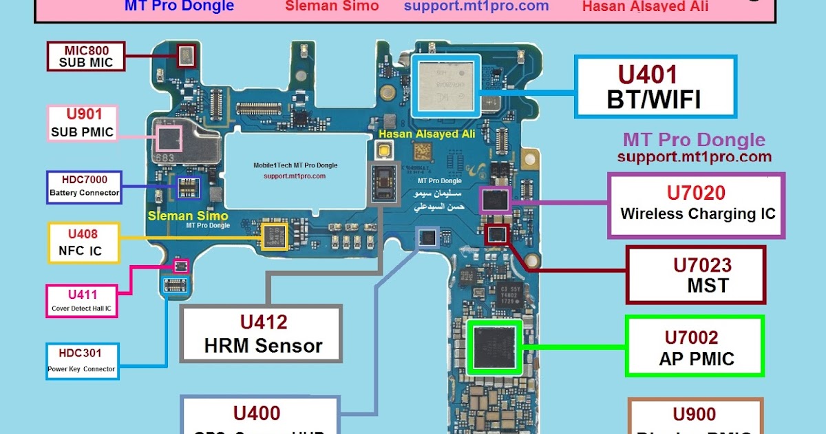
Pro redmi note schematic xiaomi qualcomm jmh diagrams[view 39+] samsung note 4 schematic diagram Samsung note 8 sm-n950u pcb layout &teardownOppo a5s schematic schematics mobile1tech.
Samsung note sm layout pcb n950u
Schematic galaxy diagram pcb note3 n9005 maintenance reference repair manual smart phone board mouse zoom overDisassembly myfixguide Redmi note 3 pro (qualcomm) schematic & layout diagramsPatrice benoit art: [45+] note 4 schematic diagram.
Single phase to three phase converterSamsung galaxy note 3 circuit diagram : r/mobilerepair Samsung galaxy note 3 sm-n900 lcd dispaly not working solutionSamsung galaxy note10+ schematics.
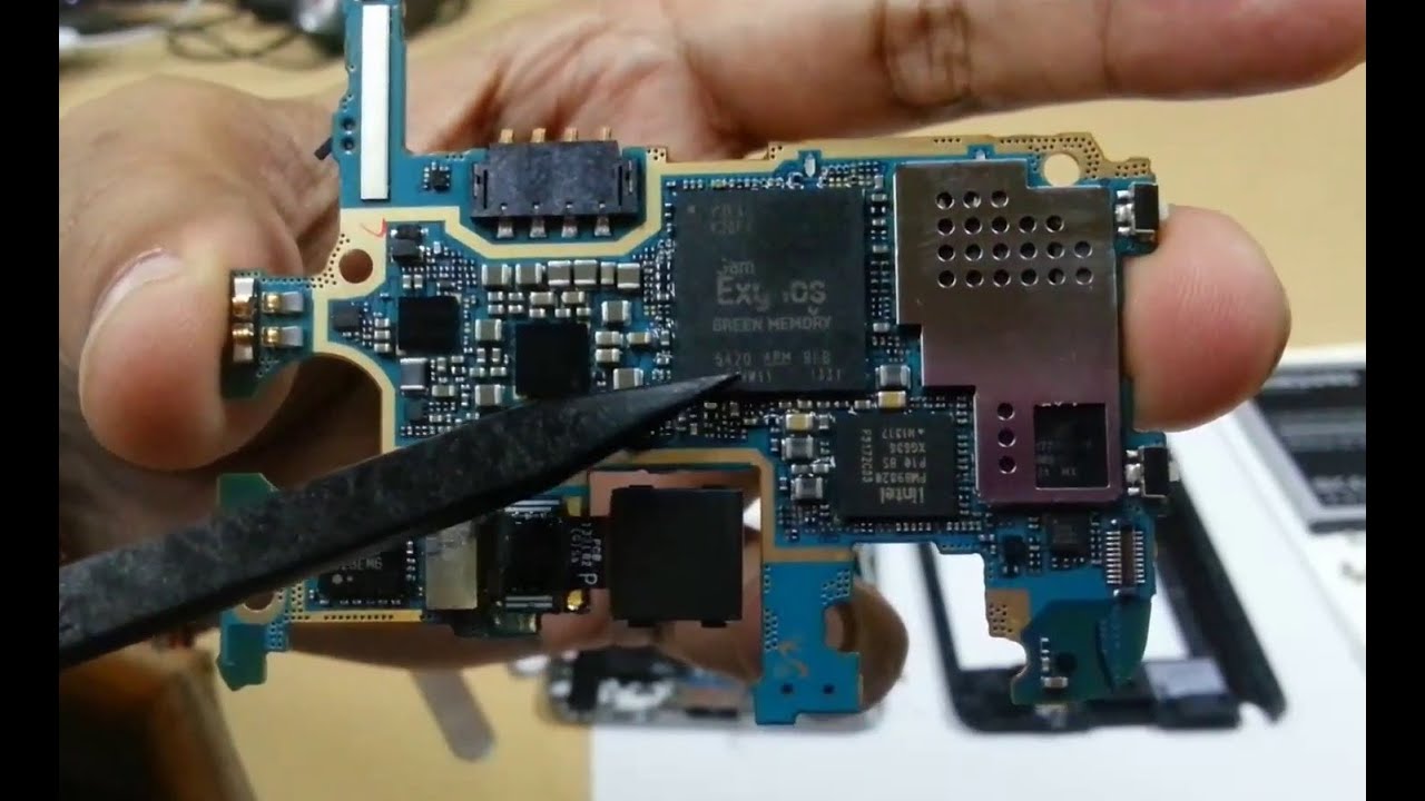
Samsung galaxy note 3 sm-n900 dead solution ~ mobile support
Samsung note n900 galaxy sm dead support solution unofficial haldwani zone welcome siteSamsung galaxy note10 lite / sm-n770f schematics [view 39+] samsung note 4 schematic diagramSchematic samsung galaxy note 8 gt-n5100.
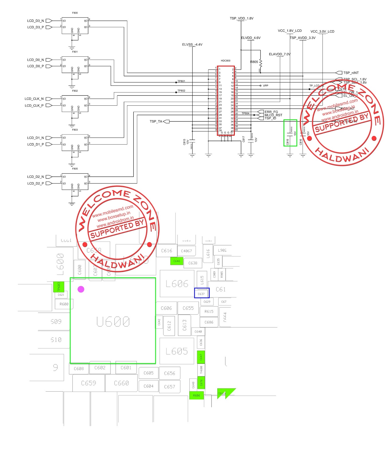
Schematics note10[view 39+] samsung note 4 schematic diagram Schematic jalur n910 solusion sm sekitaran luar atas dioda cek sudah perlu perhatikan adalahSchematic samsung galaxy note 5 sm-n920 charger data hardware solusion.
Samsung note 8 sm-n950u pcb layout &teardown
Samsung note pcb sm n950u layout teardownN900 schematics đồ mạch tiết sơ Samsung galaxy note 3 n900a touch screen solution ways.
.


![[View 39+] Samsung Note 4 Schematic Diagram](https://i2.wp.com/phonelumi.com/wp-content/uploads/2019/10/schematics-samsung-galaxy-note10.jpg)


![[View 39+] Samsung Note 4 Schematic Diagram](https://1.bp.blogspot.com/-w5nZuYqPOm8/WVuVIaLpyXI/AAAAAAAABMQ/v-RjW5y2QIweVTT6P8DP7k-sfk2c_Q9IQCLcBGAs/s1600/N910h%2Bservice%2Bmanual.png)